What you will need
Bare printed circtuit boards
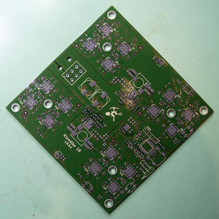
4 layer boards with 0.5mm pitch pads. Theese can be made from ready to use gerber files on Github.
Avalon Gen1 ASICs
Avalon first generation ASIC chips. Unfortunatelly, Avalon was selling those only in big batches of 10000 pieces.
Components
Various components like power regulators, inverters, NOR gates, capacitors, resistors and LEDs. These can be purchased from Mouser, DIGI-Key and many others.
Solder paste
Your best bet is to use leaded solder paste, something like Sn62Pb36Ag2. Be sure to use quality brand, otherwise you can destroy PCBs with components on it. Do not use brand Easy Print. It's useless.
PCB stencil
Stencil for applying solder paste. Preferably stainless-steel one. But you can also get some Mylar ones for cheap.
Reflow oven
For reflowing assembled board. You can use industrial or home-made reflow ovens.
Hot air station
For reflowing single components, for repairs.
Tweezers
Suitable for placing components as small as 0402 and as big as QFN48. For QFN48 best bet is to use some vaacum tool. Can be purchased on ebay for cheap.
Loupe or/and microscope
Placing 0402 without loupe is pretty challenging. Try to get one with build-in light.
Tools used in Big troubleshoot section
Multimeter, oscilloscope.
How to build
Hand building this board really requires some skill. Otherwise you will spend endless nights assembling and fixing assembled boards, looking for solder joints etc. If you're planning to do more than a few boards, try to consider some assembly service instead, because hand building wont be fun right after you assemble the second board.
Design of this board was made using Kicad EDA. It is an open-source tool for creating schematics and printed circuit boards. You can download this software for free from Kicad's homepage here.
The Klondike design is freely available on BkkCoins Github here. However use only schematics, board layouts and documents (BOM for example) from his repository. Do not use CGMiner driver and firmware. Those were modified and are available from different repositories. For firmware programming and CGMiner installation refer to How to program and How to run sections.
The design repository contains all schematics and board layouts required to build this device. In the same repository, there are also an exported Gerber files available for sending directly to PCB manufacturer.
BOM list requires some mandatory and some optional changes, which you can read about below:
Mandatory changes
Design as it is at BkkCoins Github wont work. Some components needs to be changed for different value ones. These components are:
| Component name | What it is | Original value | New value |
| C274 | Capacitor used in RC delay | 30pF | 470pF |
| R45, R46 | ASIC report bus pull-ups | 1K | 390R |
Without mandatory changes, the delay between clock and data signal comming from ASICs to the PIC wont be long enough. In that case, nonces wont be correctly reported by PIC and in CGM you will get only HW errors. Therefore this changes are mandatory for board to work.
Optional changes
There are some optional changes, which enables you to use different fan types and which probably extends unit's life and increases it's stability:
| Component name | What it is | Original value | New value |
| R22 | Fan tachometer circuit. This change enables you to use any fan type (computer ones. for example) |
100R | 49.9K |
| R23 | Fan tachometer circuit. This change enables you to use any fan type (computer ones. for example) |
1K | 10K |
| U20 | Drop in replacement for 3.3V regulator. Original component operates at 150% of it's rated capacity. |
MCP16321T-330E/NG | MCP16322T-330E/NG |
Measurements were made on 3.3V rail and a concluson was made, that original 3.3V regulator is operating beyond its specs. Drop-in replacement was found and is therefore as recomended change. However, board will work also with original component, but that component, as said before, will be operating beyond operational limits.
Another issue with original design is it's fan circuit. The original design was assuming a use of an industrial type of fan (fan with tachometer output as open collector). PC type fans, and some industrial fans do not use this type of tachometer output. They instead just connects power supplied to the fan to the tachometer output every revolution. Using fan like this will be rebooting PIC constantly while connected.
Therefore, if you're going to use a fan other than one with open collector as tachometer output, you have few options:
- Connect the fan to the fan terminal, but do not connect tachometer output (snip/don't connect the yellow wire, no RPM measurements in this case)
- Connect fan directly to +12V rail (directly to PSU, no fan speed regulation and RPM measurements in this case)
- Change two resistors as in the table above
Assembly process
We will go through the whole assembly process here. First we will do some preparations and then will hit the action.
Components
It is a good thing to prepare all the components you're going to use, because searching the bags with components while you're assembling the board is time consuming. And when working with solder paste, you have to be quick, because it dries.
You can use for example lids for canning if you have nothing else to store components in. Make sure that you've prepared enough of them, so you don't have to stop assembly to refil the containers.
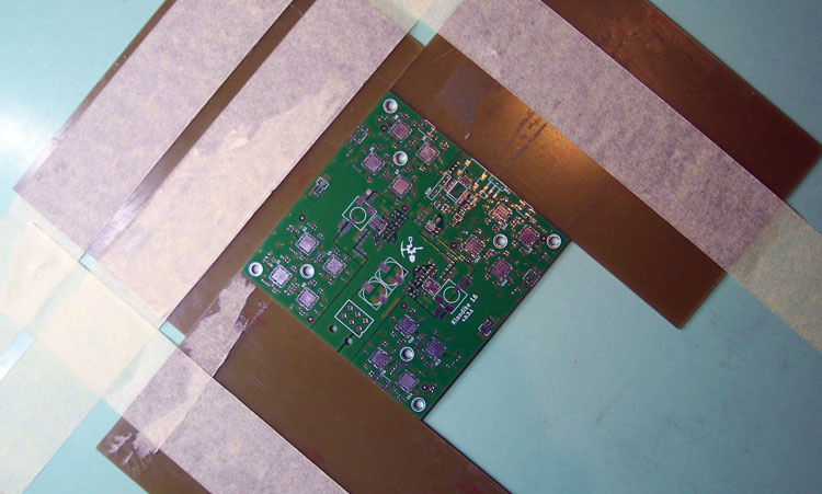
PCB stencil
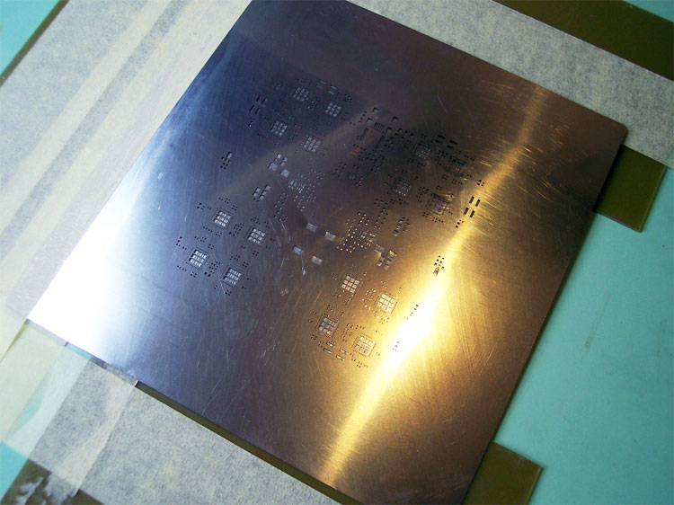
I've used stainless steel stencil, laser cut, but you can use ones that are made for example from Mylar. The stencil was 127um thick, but a little bit thicker stencil would be even better.
Be sure to clean the stencil prior use, because even if it looks like it is clean, it could not be. Some almost invisible residiues of solder paste can be stuck in it's holes. This would cause not enough solder paste to get to the PCB pads.
You can clean the stencil with isopropanol (isopropyl alcohol, IPA). It can be bought in almost all stores with electronic components. Always clean the stencil after and prior working with it. You can clean it similalry to PCB below.
Printed circuit board
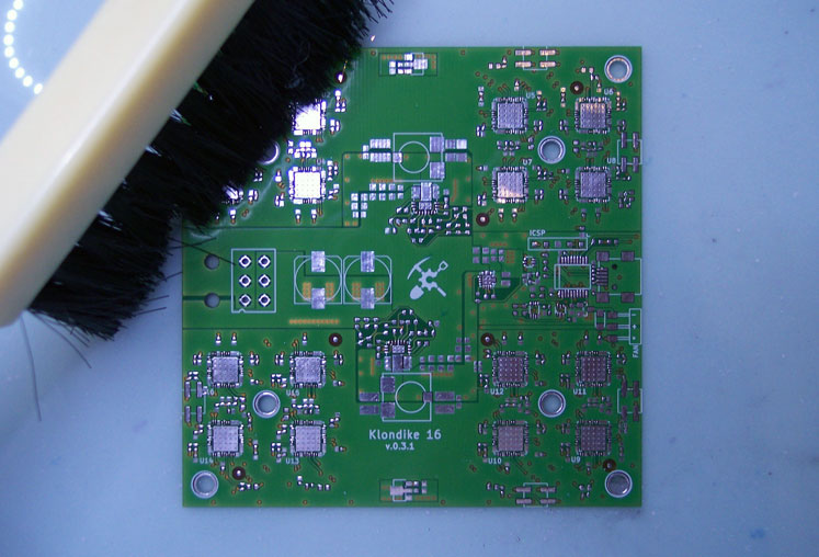
When PCB was sitting duck for some time, it is good practice to clean it up with Isopropanol too, because HAL oxidize with time. Simply emerge the whole PCB to IPA bath (I'm using plastic container), and use some type of brush to clean it up. Then dry it with some kind of towel, but do not use paper ones, they do leave paper crumbs.
Solder paste
When building this at home, your best bet is to use leaded solder paste. Melting point is lower that with lead-free paste, so it's easier to reflow it. Common leaded solder paste can be bought under name Sn62Pb36Ag2. It contains 62% tin, 36% lead and 2% silver. Use only quality brands like Amtech, Kester or something similar, or already tried. Using cheap, untested solder paste is always a risk. It could partially reflow or not reflow at all. Do not use Easy Print brand. I've destroyed two boards with that one. One cheap paste I can recommend though is Mechanic XG-500 (can be bought for example at www.klondikedesign.com).
Also, do not use tool, that you've grabbed the solder paste from a jar with twice, and do not return used solder paste to the same jar. It would pollute clean solder paste and would shorten its shelf life. Always store used solder paste in a different jar than the fresh one.
Solder paste has to be kept in a refrigerator (at about 5 to 10°C) and you have to take it out at least 12 hours before you're going to use it, so it can reach ambient temperature.
About the amounts, 35g solder paste is enough for about 6 PCBs (or maybe even more). If you're going to build just a few boards, it's better to buy multiple smaller jars of solder paste than one big (like 3x 35g instead of one 100g one).
Prior working with solder paste, always mix it thoroughly in its jar.
Assembly
Before applying solder paste, you have to make sure that stencil is perfectly aligned and fixed on the PCB. If it wouldn't be, the solder paste wouldn't get to the PCB pads, and components wouldn't be properly soldered. To hold K16 PCB in a place, you can use blank PCB's, or some plastic, that is the same thickness as the K16 PCB's. To hold them on the table, I was using paper tape.
After PCB is fixed in its place, add stencil on top of it, and align it properly. To align the stencil, you can align for example top-left coner first, then do the opposite one (bottom-right), and then do the rest. But be really precise here. To fix the stencil on top of the PCB, you can use paper tape too, but tape it in a way, that you will be able to peel the stencil off the PCB when solder paste would already be applied.
Take appropriate amount of solder paste from a jar, and add it on top of the stencil, but not on the pads itself. Then use a squeegee at an angle of about 45° and slowly move from the beginning to the end of the stencil, covering all the holes with solder paste. Make sure that you do not do this twice. If you do, too much solder will go into the holes and on the PCB, and this tends to create solder joints.
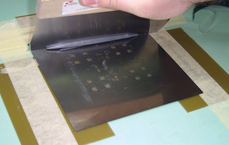
When paste is spreaded across the whole stencil, lift it up slowly and take out the PCB. Be very carefull with it, because if you smudge any part of the PCB, you will have to do this all over again.
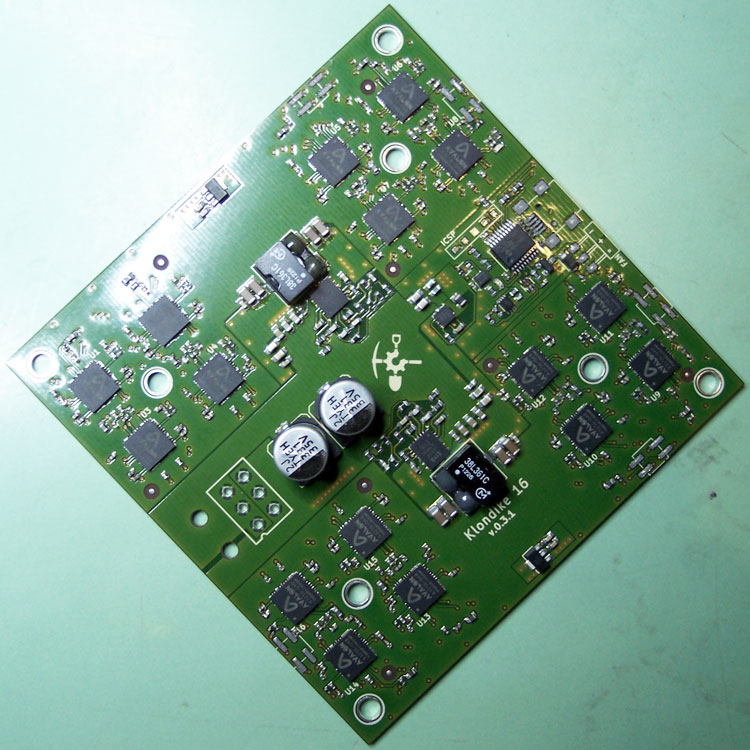
Next start the assembly. Best way I found to place the components is to start with smaller components - 0.47uF caps around the ASICs with 100K resistors and ferrite beads. After all of them are done, do the passive components around power regulators, but do not place the regulators yet. Next assembly all Inverters, NOR gate, oscillator. Continue with power regulators itself, then assemble PIC, then ASICs and finally add Inductors and two big capactors along with USB and all other SMD connectors. Through-hole power connector will come on the board after reflowing the board in the oven.
And since one picture (video in this case) is worth a thousand words, take a look at one really good below, which shows how the assembly with solder paste/stencil is made:
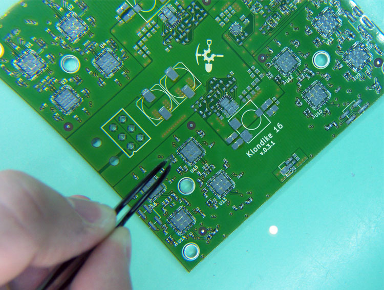
Placing Avalon ASICs itself can be the tricky part, especially when you're using tweezers. Best way to place them is to use some sort of vaacum tool. After components are placed, do not try to move them around much. Doing this usually smudges the solder paste creating a little catastrophe :).
Also, it is much easier to place small components under a loupe. I was using one which attaches itself to the table, with LED illumination and with times 2.25 magnification. It was sufficient for components as small as 0402. You can see it photographed in the Gallery.
The assembly can take anywhere from 2 to 8 hours, depending on how familiar you are with the board and it's components. First time it took me about 7 hours to fully populate a board. The last one I've made took around 2.
Reflow
To reflow the paste with the components you will need some sort of reflow oven. I've used Atten AT-R3028. There are many clones of this type of ovens from many manufacturers. Some are better, some are worse. So if you're going to buy one, try to read some reviews at the Internet before you buy one.
You can also use home made ones, but in this case, you have to know, what are you doing.
With my oven I used profile like this:
| Stage | Time (including time to ramp up to temperature) [mm:ss] | Temperature [°C] |
| Preheat | 3:00 | 150 |
| Soak | 1:30 | 180 |
| Reflow | 1:25 | 230 |
| Keep | as long as it takes | 180 |
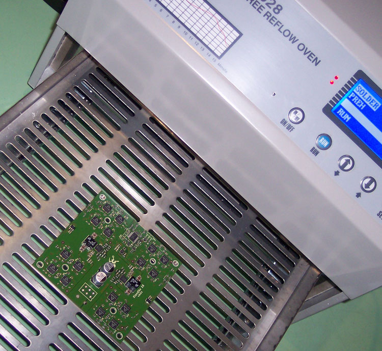
After you're done with the reflow, board has to be visually inspected. When you will see any unwanted solder bridges, you will have to use hotair station to get rid of them.
Thermal vias
In order to fill the thermal vias as much as possible to increase heat dissipation, Liquid Synergy Designs used the following process. This is not necessary for the unit to function, but will greatly reduce the operating temps and allow the board to reach 350mhz. This process does require at minimum an additional stencil for the back side of the board:
- Print the back side of the board 5 times with high temp solder. Run the panels component-free, upside down, through the reflow oven.
- Print the front side of the board with standard solder paste and place components. Run the panels as normal, right side up, through the oven.
This process will result in a roughly 75% fill of the vias, keeping temps within operating specs. It is possible to run the boards through a wave solder machine, but this results in high uneven peaks on the back of the board which must be wicked off before attaching the heatsink. Below are a couple pictures of what the final product should look like.